Description
We provide the world's largest size commercially available GeSe crystals at the highest quality GeSe and affordable prices. World's only commercial high grade Bridgman GeSe crystals measure 0.6-1.2cm in size and exhibits clean cleavable surfaces. CVT grown lower grade crystals measure more in weight but has lower crystalline quality.
Description
Germanium selenide (GeSe) is a 2D layered semiconductor wherein each individual GeSe layers are bonded through weak van der Waals (vdW) interactions. Our single crystal GeSe crystals come with guaranteed optical, electronic, and structural anisotropy. GeSe crystals are developed at our facilities using state-of-art flux zone techniques. Each growth takes close to three months to provide you perfected crystals that does not contain any halides. Each crystal is highly crystalline, oriented in 0001 direction, and easy to exfoliate. Our R&D staff takes characterization dataset in each sample piece to ensure structural, optical, and electronic consistency.
GeSe Characteristics
| Sample size | Many 4-5 mm sized crystals reaching 0.5 to 1 grams. If your research needs larger amounts please reach us |
| Material properties | High mobility IR semiconductor |
| Crystal structure | Orthorhombic phase |
| Degree of exfoliation | medium hard to exfoliate |
| Production method | Flux zone growth (6N pure) [CVT optional at 5.6N pure] |
| Other characteristics |
|
Growth method matters
What's the difference between Flux zone and CVT growth method? Contamination of halides and point defects in layered crystals are well known cause for their reduced electronic mobility, reduced anisotropic response, poor e-h recombination, low-PL emission, and lower optical absorption. Flux zone technique is a halide free technique used for synthesizing truly semiconductor grade vdW crystals. This method distinguishes itself from chemical vapor transport (CVT) technique in the following regard: CVT is a quick (~2 weeks) growth method but exhibits poor crystalline quality and the defect concentration reaches to 1E11 to 1E12 cm-2 range. In contrast, flux method takes long (~3 months) growth time, but ensures slow crystallization for perfect atomic structuring, and impurity free crystal growth with defect concentration as low as 1E9 - 1E10 cm-2. During check out just state which type of growth process is preferred. Unless otherwise stated, 2Dsemiconductors ships Flux zone crystals as a default choice.
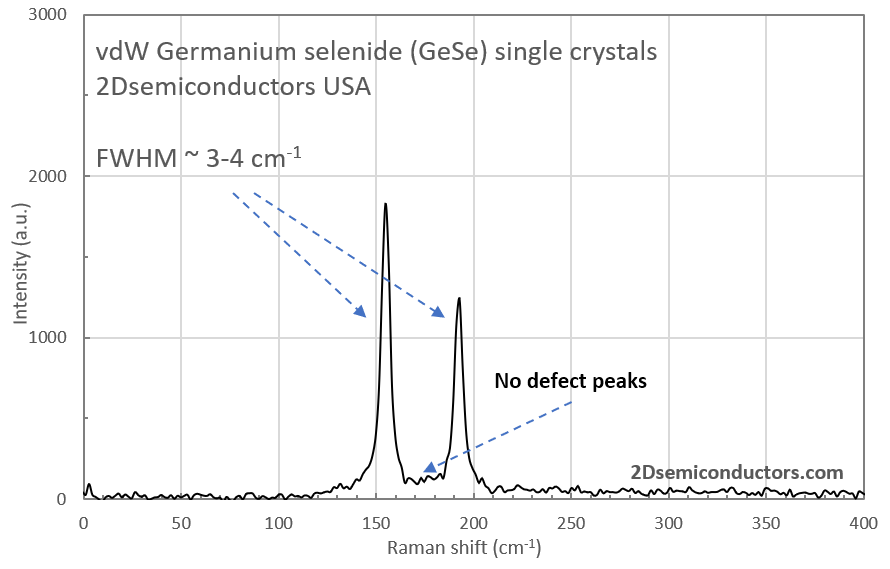
Raman spectrum collected from GeSe vdW crystals using 532 nm excitation laser

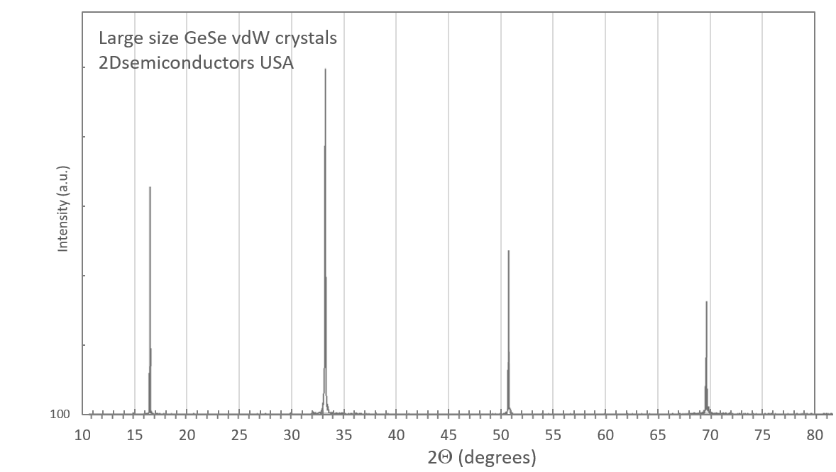
XRD Data taken from GeSe vdW Crystals

References
Functional Monochalcogenides: Raman Evidence Linking Properties, Structure, and Metavalent Bonding
Christophe Bellin, Amit Pawbake, Lorenzo Paulatto, Keevin Béneut, Johan Biscaras, Chandrabhas Narayana, Alain Polian, Dattatray J. Late, and Abhay Shukla
Phys. Rev. Lett. 125, 145301 (2020)
Additional Information
Elements: |
Ga,Se |
Element: |
Gallium |
Element: |
Selenium |
Formula: |
GaSe |
Material class: |
MX |
Properties: |
Semiconductor |
Band gap range: |
VIS |
Growth method: |
Bridgman |
Growth method: |
CVT |
Doping: |
Undoped |
Doping: |
p-Type |
Doping: |
n-Type |


