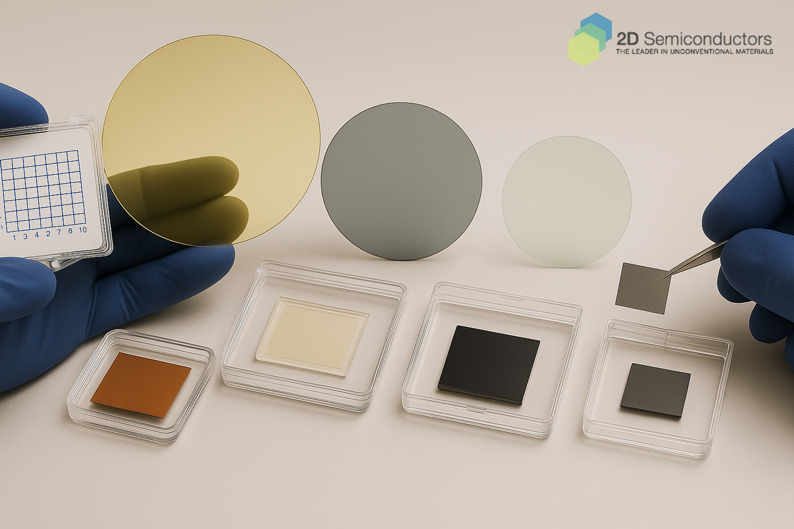
2D MBE MONOLAYERS
Molecular beam epitaxy (MBE) growth is considered as one of the most sophisticated techniques for epitaxial synthesis of high quality optical, electronic, quantum, and thermal grade materials. The true power of this technique comes from our ability to send very slim amount of atoms (as low as 5 atoms per second) onto atomically flat substrates to reach high crystallinity. Entire growth takes place at pressures as low as 1E-9 Torr to create high quality and pure materials.
Currently, our team offers MoS2, MoSe2, WS2, and WSe2 monolayers onto sapphire in our two MBE deposition chambers. In the near future, our deposition team will offer these materials on conductive substrates such as graphite and gold for scanning tunnelling microscopy (STM) studies. Within 2019, we envision releasing new MBE grown materials including, SnS2, SnSe2, PtS2, PtSe2, PdS2, PdSe2, ZrS2, and ZrSe2. In teh beginning of 2020, our company intends to release MBE grown quantum materials for more advanced measurements and tests.
Average structural comparison between MBE, CVD, and MOCVD grown samples