Description
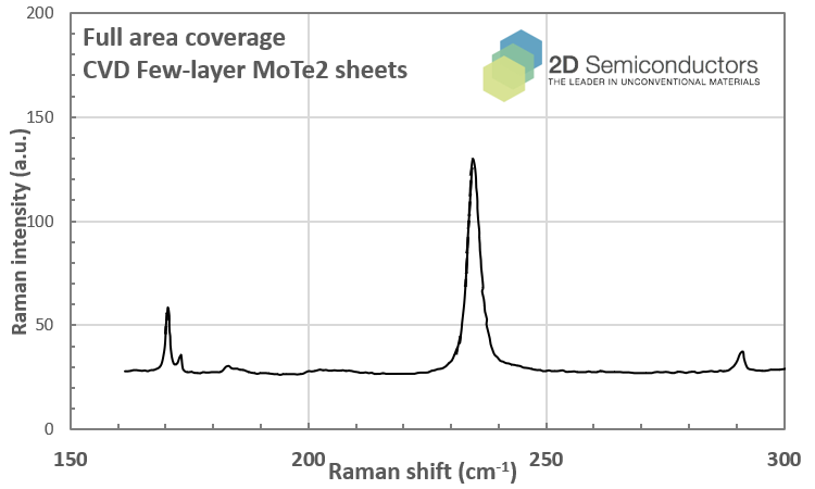
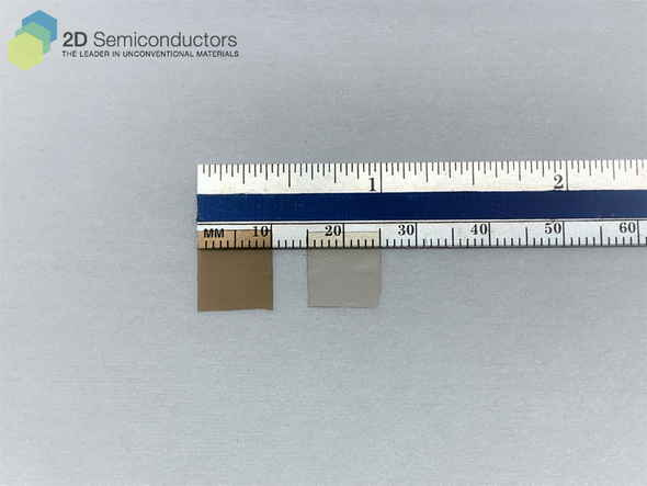
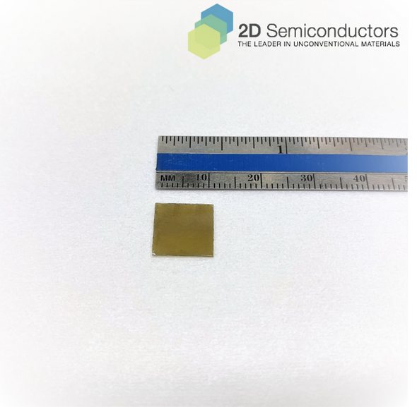
2H semiconducting phase few-layer MoTe2 (3-6 layers) has been grown on 1cm2 size c-cut sapphire substrates using low-pressure chemical vapor deposition technique (LPCVD). Grown sheets can also be transferred onto other substrates such as quartz, SiO2/Si, PET, metals, and others on request. Few-layer MoTe2 reach full area coverage on sapphire, exhibit outstanding environmental stability, surface smoothness, and uniformity. Grown sheets are environmentally stable and exhibit band gap between bulk (0.6 eV) and monolayer (1.1 eV).
Special note: Despite extensive R&D efforts, CVD grown monolayer MoTe2 are environmentally rather unstable due to uncontrollable defect characteristics. We are unable to provide monolayer thick MoTe2 at this time.
Growth method: Our company synthesizes these few layers using chemical vapor deposition (CVD) using highest purity (6N) gases and precursors in semiconductor grade facilities to produce crystalline and large domain size samples (1-50um). Other sources typically use MOCVD or sputtering process wherein defects are very large, domain sizes are small (10nm-500nm), and products are non-layered. Our samples are always highly crystallized, high purity, and perfectly layered.
Characteristics of CVD grown 2H (semiconducting phase) MoTe2 sheets by 2Dsemiconductors Inc.
| Sample size | 1cm x 1cm square shaped |
| Substrate type | c-cut sapphire (default) other substrates on demand |
| Coverage | Full-area coverage |
| Electrical properties | 0.8-1.0 eV semiconductor |
| Crystal structure | Hexagonal Phase |
| Unit cell parameters | a = b = 0.350 nm, c = 1.341 nm, α = β = 90, γ = 120° |
| Production method | Low pressure Chemical Vapor Deposition (LPCVD) |
| Characterization methods | Raman, photoluminescence, TEM, EDS |

Additional Information
Elements: |
Mo,Te |
Element: |
Molybdenum |
Element: |
Tellurium |
Formula: |
MoTe2 |
Material class: |
MX2 |
Material class: |
Dichalcogen |
Properties: |
Semiconductor |
Properties: |
Excitonic |
Band gap range: |
IR |
Growth method: |
CVD |
Doping: |
Undoped |
Thin-film type: |
Few-layer |
Substrate: |
Sapphire |
Substrate: |
Quartz |
Substrate: |
PET |
Substrate: |
Custom |


