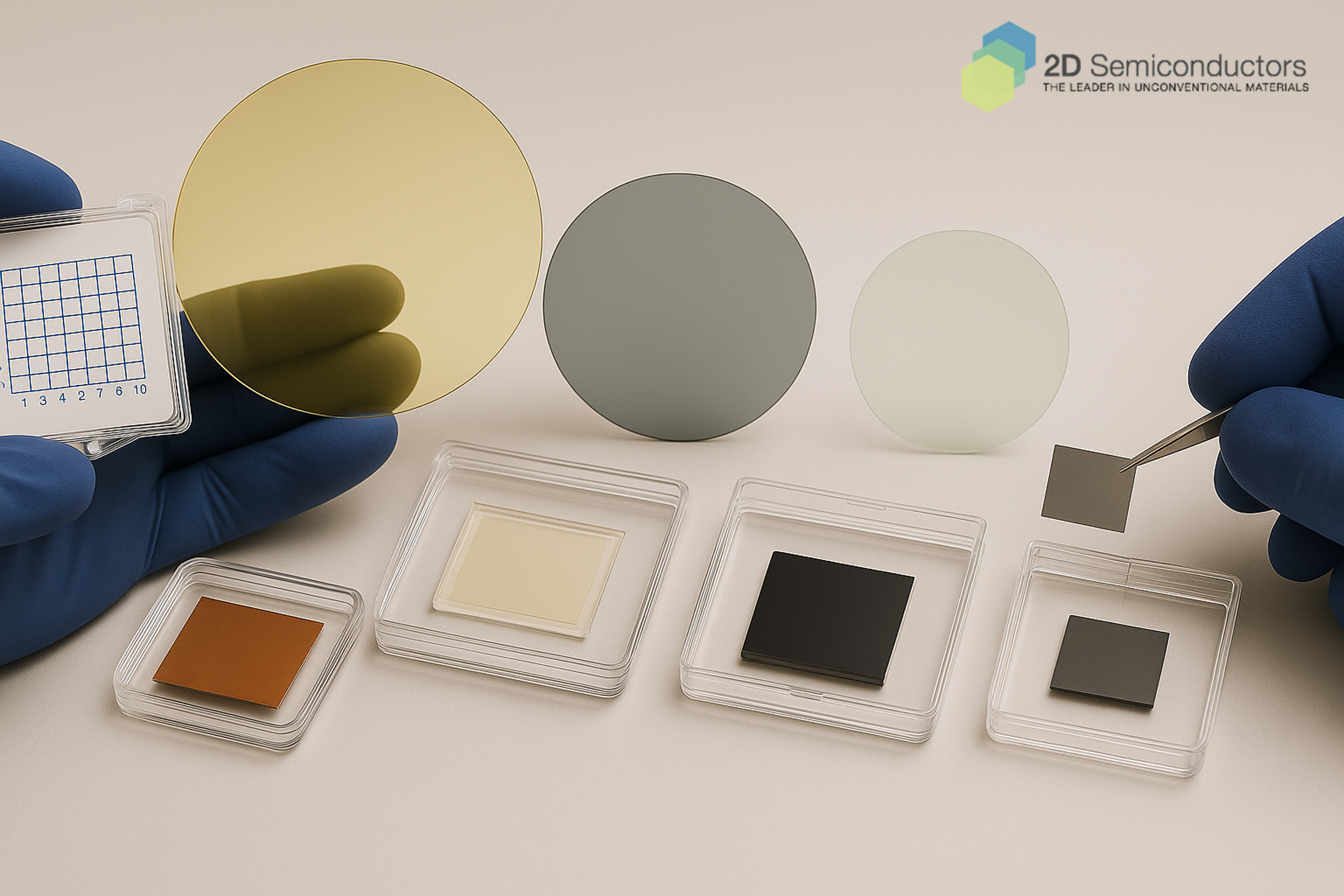
WSe2
Thickness. We offer monolayer or few-layer thick WSe2 sheets on variety of substrates. Please select from few-layer vs. monolayer WSe2 products.
On sapphire. 1cm2 size full area CVD WSe2 monolayers on c-cut sapphire and isolated single crystal WSe2 monolayer triangles on 1cm2 size c-cut sapphire substrates are listed under this category. Monolayers are highly crystalline, exhibit sharp Raman peaks, and are highly luminescent. See TEM, PL, Raman, and other datasets by clicking the product item below.
On SiO2/Si. 1cm2 size full area CVD WSe2 monolayers on SiO2/Si and isolated single crystal WSe2 monolayer triangles on 1cm2 SiO2/Si substrates are listed under this category. Monolayers are highly crystalline, exhibit sharp Raman peaks, and are highly luminescent.
Substrate type. By default, WSe2 monolayers are first grown onto sapphire and then transferred onto SiO2/Si substrates. Silicon substrates are highly doped for electronic measurements (~5E18cm-3 n-type) and SiO2 thickness at 285nm.
Substrate type and material selection. Please click on the product listed below, and use selection options to identify your material and desired substrates. If the substrate is not listed, please contact us to discuss your options.
Download the full CVD Product Catalog