Description
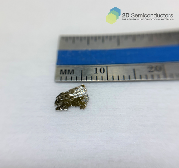
NbOCl2 crystals by 2Dsemiconductors. NbOCl2 has a layered crystal structure, with covalently bonded NbO layers and Cl ions situated in the interstitial spaces between them. NbOCl2 is a semiconductor material that exhibits an intriguing property of charge-density wave (CDW) formation and quantum light emitters. NbOCl2 has been extensively studied for its unusual electronic properties and the mechanism behind CDW formation and more recently for their quantum emitter properties. It also has potential applications in areas such as energy storage and conversion, as well as in the design of novel electronic devices.
![]() Materials Project NbOCl2
Materials Project NbOCl2
![]() C2DB material properties NbOCl2
C2DB material properties NbOCl2
The properties of NbOCl2 vdW crystals
| Sample size | ~3-6mm sized crystals |
| Material properties | Charge density wave, semiconductor, and quantum emitter |
| Crystal structure | Monoclinic (c2) |
| Degree of exfoliation | Easy exfoliation characteristics |
| Production method | Modified flux zone growth |
| Other characteristics |
|
Additional Information
Elements: |
Nb,O,Cl |
Element: |
Niobium |
Element: |
Oxygen |
Element: |
Chlorine |
Formula: |
NbOCl2 |
Material class: |
Oxide |
Material class: |
Halide |
Material class: |
Quasi-1D |
Properties: |
Semiconductor |
Properties: |
CDW |
Band gap range: |
VIS |
Growth method: |
Flux |
Doping: |
Undoped |


