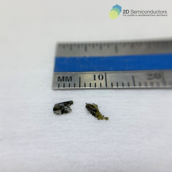
Description
ZrGeTe4 crystal is a layered anisotropic semiconductor with the predicted bandgap of 0.4 eV. While it is layered and can be exfoliated down to few- and monolayers, their properties remain largely unknown. Our ZrGeTe4 vdW crystals are synthesized using flux zone growth technique at unparalleled 99.9999% confirmed purity rates. Crystals are cut in c-axis and thus are ready to exfoliate onto desired substrates.
Summary of ZrGeTe4 vdW crystals
| Sample size | ~4-5mm in size |
| Material properties | 2D anisotropic IR semiconductor |
| Crystal structure | Tetragonal phase |
| Unit cell parameters | a=b=0.382 nm, c=0.911 nm, α=β=90°, γ=120° |
| Production method | Flux zone |
| Characterization methods | SIMS, XRD, EDS |
Publications
Visible to Short-Wave Infrared Photodetectors Based on ZrGeTe4 van der Waals Materials
ACS Appl. Mater. Interfaces 2021, 13, 38, 45881–45889
Additional Information
Elements: |
Zr,Ge,Te |
Element: |
Zirconium |
Element: |
Germanium |
Element: |
Tellurium |
Formula: |
ZrGeTe4 |
Material class: |
MX4 |
Material class: |
Tetrachalcogen |
Material class: |
Quasi-1D |
Properties: |
Semiconductor |
Band gap range: |
Unknown |
Growth method: |
Flux |
Doping: |
Undoped |


