Description
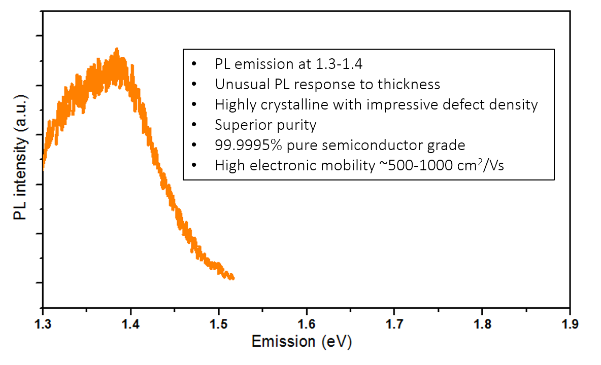
Bismuth sulfide (Bi₂S₃) Developed at our facilities in the last five (5) years to optimize the perfect stoichiometry. Bi2S3 has layered (lamellar) structure much similar to other 2D crystals such as graphite, MoS2, and Sb2Te3. They can be exfoliated down to monolayers through standard mechanical exfoliation technique. Bi2S3 is stabilized in orthorhombic phase and has semiconducting behavior (~1.35 eV gap). Bi2S3 crystals come with perfect 0001 basal plane cleavage meaning it is ready for exfoliation without any further processing. The crystals were characterized and confirmed by x-ray diffraction (XRD), x-ray photoelectron spectroscopy, Raman, photoluminescence, SIMS, and Auger electron spectroscopy techniques.
Properties of vdW Bi2S3 crystals
| Sample size | Centimeter scale |
| Material properties | Semiconductor |
| Crystal structure | Monoclinic phase |
| Unit cell parameters | a=0.403, b=1.113 nm, c=1.138 nm, α=β=90° |
| Growth method | [Default] Bridgman growth technique (structurally perfect) [Optional] Flux zone (no halide contamination) defect free |
| Purity | 99.9999% confirmed |
XRD data from Bi2S3 crystals

Raman spectrum from Bi2S3 crystals - 2Dsemiconductors USA

PL spectrum from Bi2S3 crystals - 2Dsemiconductors USA

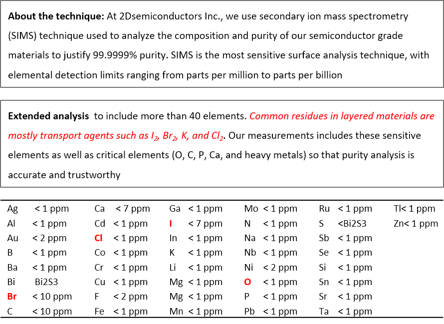
Purity analysis (SIMS) from Bi2S3 crystals - 2Dsemiconductors USA

Additional Information
Elements: |
Bi,S |
Element: |
Bismuth |
Element: |
Sulfur |
Formula: |
Bi2S3 |
Material class: |
M2X3 |
Properties: |
Semiconductor |
Band gap range: |
VIS |
Growth method: |
Bridgman |
Growth method: |
Flux |
Doping: |
Undoped |


