


Description
h-BN (Boron Nitride) monolayer, few-layer or multilayer film is grown onto 50 um thick copper foils only on the top surface of the Cu foils. h-BN is an insulator with a direct band gap of 6 eV with strong ionic bonding between B-N atoms. Our h-BN CVD process has been adopted in order that defect density has been kept low (~1E10-1E11 cm-2) and single domain sizes have been increased to reduce 1D grain boudary defect concentrations. h-BN sheets measure ~5cm x 5cm or ~2x2 inches in size.
Properties of h-BN
| CVD h-BN | 2x2 inches on 50um thick Cu foils |
| Material properties | ~6eV gap insulator |
| Crystal structure | Hexagonal phase |
| Growth method | Chemical vapor deposition (CVD) |
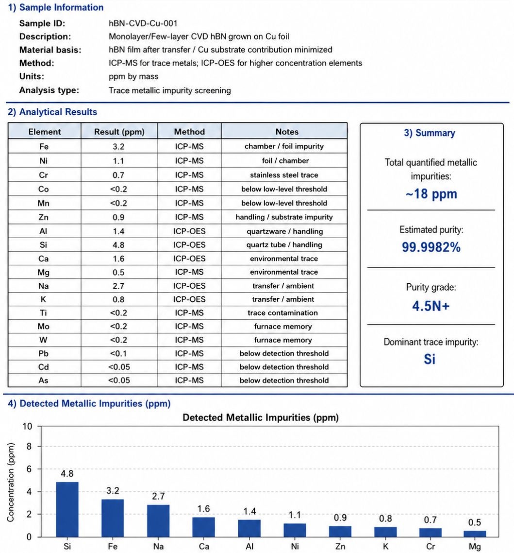
Unmatched purity
Raman spectra from h-BN monolayer thick films

TEM images collected from h-BN sheets suspended on TEM grids

Additional Information
Elements: |
B,N |
Element: |
Boron |
Element: |
Nitrogen |
Formula: |
BN |
Material class: |
Nitride |
Properties: |
Insulator |
Properties: |
Excitonic |
Band gap range: |
UV |
Growth method: |
CVD |
Doping: |
Undoped |
Thin-film type: |
Monolayer |
Thin-film type: |
Few-layer |
Thin-film type: |
Multilayer |
Substrate: |
Copper foil |


