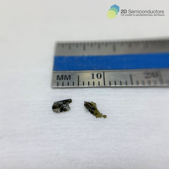
GeS crystals - 1 cm size high quality GeS germanium sulfide crystals by 2Dsemiconductors USA GeS crystals - 1 cm size high quality GeS germanium sulfide crystals by 2Dsemiconductors USA GeS crystals - 1 cm size high quality GeS germanium sulfide crystals by 2Dsemiconductors USA PL spectrum from GeS crystals - 1 cm size high quality GeS germanium sulfide crystals by 2Dsemiconductors USA Raman spectrum from GeS crystals - 1 cm size high quality GeS germanium sulfide crystals by 2Dsemiconductors USA Properties of GeS crystals - 1 cm size high quality GeS germanium sulfide crystals by 2Dsemiconductors USA XRD data taken from bulk GeS vdW crystals by 2Dsemiconductors USA Surface morphology of GeS crystals by 2Dsemiconductors USA

Germanium Sulphide (GeS)

SKU: BLK-GeS
$580.00

We provide the world's largest size commercially available GeS crystals at the highest quality GeS and affordable prices. Our crystals exceed competing crystals both in size and quality.

Description

(Germanium sulfide) is a 2D semiconductor with 1.65 eV band gap in the bulk form. They exhibit strong in-plane crystalline anisotropy giving rise to highly anisotropic excitons, high carrier mobility channels, and thermal conduction pathways. Theoretically it has been predicted to undergo a structural phase transition around 400 C. Our single crystal GeS (Germanium sulfide) crystals come with guaranteed optical, electronic, and structural anisotropy. They are developed at our facilities using state-of-art flux zone techniques. Each growth takes close to three months to provide you perfected crystals that does not contain any halides. Each crystal is highly crystalline, oriented in 0001 direction, and easy to exfoliate. In the bulk form GeS is 1.65 eV indirect band gap semiconductor. Displays remarkable and unusual optical, mechanical, and electrical properties in the monolayers. Monolayer GeS remains unknown by the scientific community and waiting to be discovered. Our R&D staff takes characterization dataset in each sample piece to ensure structural, optical, and electronic consistency. Please also see our GeSGeSeGeTeGeAsGeP, and Ge-based solutions.

Monolayer GeS solutions are also available here

GeS characteristics

ges-properties-2.png

Growth method matters> Flux zone or CVT growth method? Contamination of halides and point defects in layered crystals are well known cause for their reduced electronic mobility, reduced anisotropic response, poor e-h recombination, low-PL emission, and lower optical absorption. Flux zone technique is a halide free technique used for synthesizing truly semiconductor grade vdW crystals. This method distinguishes itself from chemical vapor transport (CVT) technique in the following regard: CVT is a quick (~2 weeks) growth method but exhibits poor crystalline quality and the defect concentration reaches to 1E11 to 1E12 cm-2 range. In contrast, flux method takes long (~3 months) growth time, but ensures slow crystallization for perfect atomic structuring, and impurity free crystal growth with defect concentration as low as 1E9 - 1E10 cm-2. During check out just state which type of growth process is preferred. Unless otherwise stated, 2Dsemiconductors ships Flux zone crystals as a default choice. 

Germanium sulfide (GeS) XRD characterization

ges-xrd.png

SEM images taken from Germanium sulfide crystals

ges-sem-images.png


Germanium sulfide Raman spectroscopy data at different polarization angles (showing angular dependence)

ges-raman.png


Photoluminescence data collected from GeS crystals (magenta bulk GeS, black 3L GeS)

ges-pl-data.png


Full Description
Formula: GeS
Qty
  • Description

    Germanium Sulphide (GeS)

    We provide the world's largest size commercially available GeS crystals at the highest quality GeS and affordable prices. Our crystals exceed competing crystals both in size and quality.

    Description

    (Germanium sulfide) is a 2D semiconductor with 1.65 eV band gap in the bulk form. They exhibit strong in-plane crystalline anisotropy giving rise to highly anisotropic excitons, high carrier mobility channels, and thermal conduction pathways. Theoretically it has been predicted to undergo a structural phase transition around 400 C. Our single crystal GeS (Germanium sulfide) crystals come with guaranteed optical, electronic, and structural anisotropy. They are developed at our facilities using state-of-art flux zone techniques. Each growth takes close to three months to provide you perfected crystals that does not contain any halides. Each crystal is highly crystalline, oriented in 0001 direction, and easy to exfoliate. In the bulk form GeS is 1.65 eV indirect band gap semiconductor. Displays remarkable and unusual optical, mechanical, and electrical properties in the monolayers. Monolayer GeS remains unknown by the scientific community and waiting to be discovered. Our R&D staff takes characterization dataset in each sample piece to ensure structural, optical, and electronic consistency. Please also see our GeSGeSeGeTeGeAsGeP, and Ge-based solutions.

    Monolayer GeS solutions are also available here

    GeS characteristics

    ges-properties-2.png

    Growth method matters> Flux zone or CVT growth method? Contamination of halides and point defects in layered crystals are well known cause for their reduced electronic mobility, reduced anisotropic response, poor e-h recombination, low-PL emission, and lower optical absorption. Flux zone technique is a halide free technique used for synthesizing truly semiconductor grade vdW crystals. This method distinguishes itself from chemical vapor transport (CVT) technique in the following regard: CVT is a quick (~2 weeks) growth method but exhibits poor crystalline quality and the defect concentration reaches to 1E11 to 1E12 cm-2 range. In contrast, flux method takes long (~3 months) growth time, but ensures slow crystallization for perfect atomic structuring, and impurity free crystal growth with defect concentration as low as 1E9 - 1E10 cm-2. During check out just state which type of growth process is preferred. Unless otherwise stated, 2Dsemiconductors ships Flux zone crystals as a default choice. 

    Germanium sulfide (GeS) XRD characterization

    ges-xrd.png

    SEM images taken from Germanium sulfide crystals

    ges-sem-images.png


    Germanium sulfide Raman spectroscopy data at different polarization angles (showing angular dependence)

    ges-raman.png


    Photoluminescence data collected from GeS crystals (magenta bulk GeS, black 3L GeS)

    ges-pl-data.png