Description
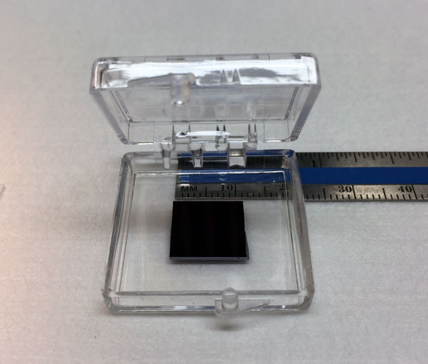
Monolayer, Few-layer or multilayer hBN transferred on SiO2/Si substrates. Full area hBN layers were synthesized first using our established CVD growth method on copper foils and transferred from copper onto SiO2/Si using copper etchant and polymer assisted stamping technique. Sample size measures 1cm in size. Due to the transfer process, the transferred layers may contain natural wrinkles and missing patches in some regions. The entire process is carried under Argon backfilled glovebox to ensure high-quality and residue free process. The samples are always sealed under Argon and pumped down to 1E-6 Torr to deliver quality samples for your research.
If your research needs designer 2D superlattices please see our transferred monolayer product line.
Additional Information
Elements: |
B,N |
Element: |
Boron |
Element: |
Nitrogen |
Formula: |
BN |
Material class: |
Nitride |
Properties: |
Insulator |
Properties: |
Excitonic |
Band gap range: |
UV |
Growth method: |
CVD |
Doping: |
Undoped |
Thin-film type: |
Monolayer |
Thin-film type: |
Few-layer |
Thin-film type: |
Multilayer |
Substrate: |
SiO2/Si |


