Description
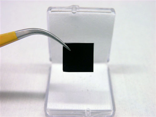
Monolayer flakes have been exfoliated from bulk crystals onto 90nm thermal oxide and measures from 5 micron up to 40 micron in size. Each sample contains at least one single-layer and is easy to find with the given x and y coordinates. Optical images and preliminary tests come with the product. Each sample is inspected under the optical microscope and x-y coordinates are recorded. Contact us for more information.
Characterization of Exfoliated Monolayers
| Exfoliated MoS₂ | Shows strong PL at 1.85-1.88 eV with 0.04 to 0.1eV FWHM. Typically, flakes show two prominent Raman peaks at 386cm-1 (E2g- in plane-) and 404cm-1 (A1g out-of-plane) and the FWHM (full-width-at-half-maximum) is less than 5cm-1. |
| Exfoliated WS₂ | Typically, single-layer WS₂ show strong PL at 2.02eV with 0.04 to 0.08eV FWHM. |
| Exfoliated WSe₂ | Typically, single-layer WSe₂ show strong PL at 1.66eV with 0.04 to 0.08eV FWHM, and the Raman peaks are located at 139.5cm-1 (E2g in-plane mode) and 249.5 cm-1 (A1g out-of-plane mode). |
| Exfoliated MoSe₂ | Typically, single-layer MoSe₂ show strong PL at 1.55eV with 0.04 to 0.07eV FWHM, and the Raman peaks are located at 287.5cm-1 (E2g in-plane mode) and 241 cm-1 (A1g out-of-plane mode). |
Possible applications:
- Electronics
- Sensors - detectors
- Optics
- STM - AFM applications
- Molecular detection - binding
- Ultra-low friction studies
- Materials science and semiconductor research
Additional Information
Elements: |
Mo,S,Se,W |
Element: |
Molybdenum |
Element: |
Sulfur |
Element: |
Selenium |
Element: |
Tungsten |
Formula: |
MoS2, MoSe2, WS2, WSe2 |
Material class: |
MX2 |
Material class: |
Dichalcogen |
Properties: |
Semiconductor |
Properties: |
Excitonic |
Band gap range: |
VIS |
Growth method: |
Exfoliated |
Doping: |
Undoped |
Thin-film type: |
Monolayer |
Substrate: |
SiO2/Si |


