Description
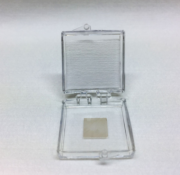
Monolayer MoSe2 transferred on SiO2/Si substrates. Full area MoSe2 monolayers were synthesized first using our established CVD growth method on c-cut sapphire and transferred from sapphire onto SiO2/Si using polymer assisted stamping technique. Sample size measures 1cm in size. Due to the transfer process, the transferred monolayers may contain natural wrinkles and missing patches in some regions. The entire process is carried under Argon backfilled glovebox to ensure high-quality and residue free process. The samples are always sealed under Argon and pumped down to 1E-6 Torr to deliver quality samples for your research.
If your research needs designer 2D superlattices please see our transferred monolayer product line [Link]
Sample Properties
| Sample size | 1cm x 1cm square shaped |
| Substrate type | Thermal oxide (SiO2/Si) substrates |
| Coverage | Full Coverage Monolayer (transfer process may create wrinkles and small missing regions) |
| Electrical properties | 1.58 eV Direct Bandgap Excitonic Semiconductor |
| Crystal structure | Hexagonal Phase |
| Unit cell parameters | a = b = 0.327 nm, c = 1.295 nm, α = β = 90°, γ = 120° |
| Production method | Atmospheric Pressure Chemical Vapor Deposition (APCVD) |
| Characterization methods | Raman, photoluminescence, TEM, EDS |
Additional Information
Elements: |
Mo,Se |
Element: |
Molybdenum |
Element: |
Selenium |
Formula: |
MoSe2 |
Material class: |
MX2 |
Material class: |
Dichalcogen |
Properties: |
Semiconductor |
Properties: |
Excitonic |
Band gap range: |
VIS |
Growth method: |
CVD |
Doping: |
Undoped |
Thin-film type: |
Monolayer |
Substrate: |
SiO2/Si |


