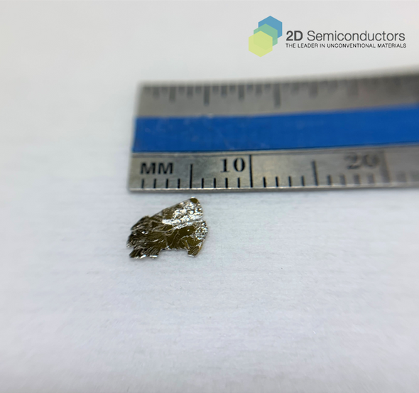
PbI2 crystals : Large size high quality 2D PbI2 crystals - 2Dsemiconductors USA PbI2 (Lead diiodide) Crystal PbI2 crystals : Large size high quality 2D PbI2 crystals - 2Dsemiconductors USA PbI2 crystals : Large size high quality 2D PbI2 crystals - 2Dsemiconductors USA PbI2 crystals : Large size high quality 2D PbI2 crystals - 2Dsemiconductors USA PL characteristics of PbI2 crystals : Large size high quality 2D PbI2 crystals - 2Dsemiconductors USA Raman characteristics of PbI2 crystals : Large size high quality 2D PbI2 crystals - 2Dsemiconductors USA

PbI2 (Lead diiodide) Crystal

SKU: BLK-PBI2
$580.00

The only commercially available lead iodide (PbI2) by 2Dsemiconductors USA. PbI2 crystallizes in a CdI2 structure, in which I- anions are packed hexagonally, and each Pb2+ cation is connected to six I- anions in alternating layers, forming a typical octahedral structure. The repeating I-Pb-I trilayer stacks in various ways and are bounded by van der Waals force, and this in return, offers a way to achieve mono- and few-layer flakes by mechanical and chemical exfoliation due to the weak interlayer forces between adjacent layers. PbI2 crystals are perfectly layered and has 2.4 eV direct band gap. Crystals arrive with perfect 0001 cleavage, and are grown by float zone technique over 4 months for perfect crystallization. PbI2 crystals are highly luminescent and arrive with guaranteed optical (photoluminescence) response.

Properties of PbI2 crystals - 2Dsemiconductors USA

Sample size ~1 cm in size
Material properties 2.4 eV band gap semiconductor (bulk)
Crystal structure CdI2 structure
Unit cell parameters a=b=0.456 nm and c=6.98 nm
Growth method Bridgman growth; optional Flux zone or chemical vapor transport
Purity 99.9999% guaranteed electronic grade
Characterization methods Raman, photoluminescence, TEM, EDS
Availability In stock

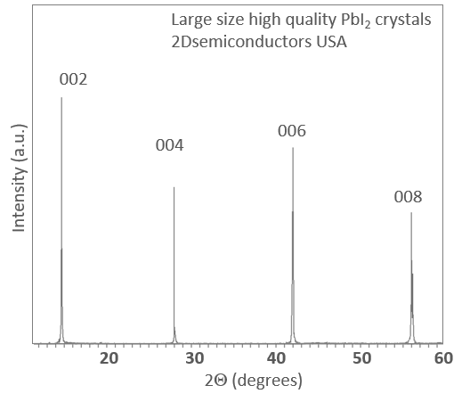
XRD data collected from PbI2 single crystals - 2Dsemiconductors USA
pbi2-xrd.png 

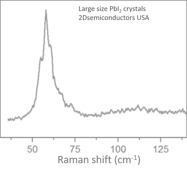
Raman spectrum collected from PbI2 crystals - 2Dsemiconductors USA
pbi2-raman.png

 PL spectrum collected from PbI2 layered crystals

pbi2-pl.png


Full Description
Formula: PbI2
Qty
  • Description

    PbI2 (Lead diiodide) Crystal

    The only commercially available lead iodide (PbI2) by 2Dsemiconductors USA. PbI2 crystallizes in a CdI2 structure, in which I- anions are packed hexagonally, and each Pb2+ cation is connected to six I- anions in alternating layers, forming a typical octahedral structure. The repeating I-Pb-I trilayer stacks in various ways and are bounded by van der Waals force, and this in return, offers a way to achieve mono- and few-layer flakes by mechanical and chemical exfoliation due to the weak interlayer forces between adjacent layers. PbI2 crystals are perfectly layered and has 2.4 eV direct band gap. Crystals arrive with perfect 0001 cleavage, and are grown by float zone technique over 4 months for perfect crystallization. PbI2 crystals are highly luminescent and arrive with guaranteed optical (photoluminescence) response.

    Properties of PbI2 crystals - 2Dsemiconductors USA

    Sample size ~1 cm in size
    Material properties 2.4 eV band gap semiconductor (bulk)
    Crystal structure CdI2 structure
    Unit cell parameters a=b=0.456 nm and c=6.98 nm
    Growth method Bridgman growth; optional Flux zone or chemical vapor transport
    Purity 99.9999% guaranteed electronic grade
    Characterization methods Raman, photoluminescence, TEM, EDS
    Availability In stock

    XRD data collected from PbI2 single crystals - 2Dsemiconductors USA

    pbi2-xrd.png 

    Raman spectrum collected from PbI2 crystals - 2Dsemiconductors USA

    pbi2-raman.png

     PL spectrum collected from PbI2 layered crystals

    pbi2-pl.png