


")
")

")


")
")

")


Description
We transfer any CVD grown monolayers onto your substrates of choice! Our R&D has developed scalable methods to transfer large area h-BN, graphene, MoS2, MoSe2, WS2, WSe2, ReS2, ReSe2, SnS2, SnSe2, PtS2, and PtSe2 sheets onto almost any substrates. Our team uses extremely delicate steps and processes to keep the 2D layers clean and unaltered. Our processes are carried out under ultra-high purity environment and inert gas glove box so that the material quality is not sacrificed. Standard samples are sapphire, SiO2/Si, SiO2 (quartz), PET flexible substrates, and sapphire. If your research needs custom substrates, this is no problem: See our word cloud listing some of the custom samples that were manufactured at our facilities. During the online check-out or when requesting a formal quote, please indicate desired substrate, and desired CVD material. Also see our work on transferred samples in the product images.
Due to highly customized nature of the process, our company does not offer refunds on these transferred samples.

Frequently asked questions
Q1: Can you transfer monolayers onto TEM grids?
A: Yes, we can transfer any CVD product onto any TEM grids. Our company requires you to select your own TEM grids, inform us the model, and send (extra) TEM grids so that we can do tests to deliver you good quality samples.
Q2: Can you guarantee that CVD monolayers will be same quality after the transfer?
A: Transfer process requires polymeric stamping and / or chemical processes. These steps generally will introduce some cracks and voids in the samples. But if you selected to transfer full area CVD monolayers, they will still be at large scales. There might be some folding, wrinkling effects, and this is normal. If your CVD monolayer is luminescent, after the transfer optical properties will remain similar with PL emission at the same wavelenghts
Q3: What kind of substrates can you transfer onto?
A: You would be surprised to know but we have transferred CVD monolayers more than 100 different substrates to date. Examples include, Bragg reflectors, plasmonic structures, SiO2/Si, sapphire, quartz, mica, PET, polymer, other 2D materials, glass, TEM grids, metals, and even on a diamond!
Q4: What is the typical processing times?
A: This will depend on your project, chemistry required, and your sets of requirements towards sample production. It is typically around 1-3 weeks.
Q5: Is it possible to return sample at a later date and request refund?
Because of the custom nature of the production process, all transferred CVD sales are final and non-refundable. Our staff uses standard CVD samples, labor, chemicals, and substrates to prepare these samples and the cost primary goes towards cost of these materials.
Recent work citing our materials
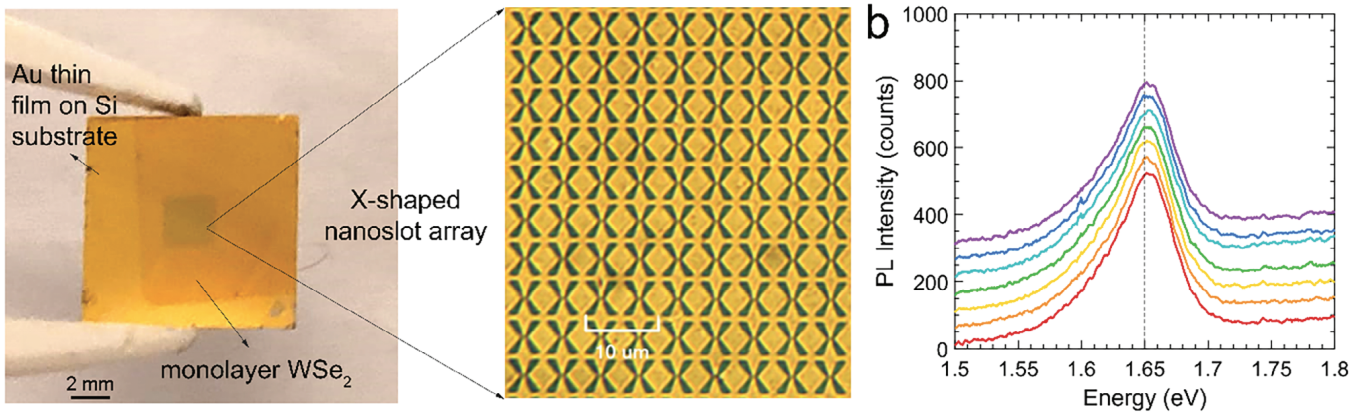
Enhanced Terahertz Spectroscopy of a Monolayer Transition Metal Dichalcogenide; Advanced Functional Materials 2025, 2419841
High carrier mobility in graphene doped using a monolayer of tungsten oxyselenide Nature Electronics volume 4, pages731–739 (2021)
X.Jin et al., Enhanced Terahertz Spectroscopy of a Monolayer Transition Metal Dichalcogenide, Advanced Functional Materials. 2025, 35, 2419841
Additional Information
Elements: |
B, N |
Elements: |
Mo, S |
Elements: |
Mo, Se |
Elements: |
Mo, Te |
Elements: |
W, S |
Elements: |
Re, S, Se |
Elements: |
Sn, S, Se |
Elements: |
Pt, S, Se |
Elements: |
Pd, S, Se |
Formula: |
MoS2 |
Formula: |
WS2 |
Formula: |
MoSe2 |
Formula: |
WSe2 |
Formula: |
MoTe2 |
Formula: |
PtS2 |
Formula: |
PtSe2 |
Formula: |
PdS2 |
Formula: |
PdSe2 |
Formula: |
ReS2 |
Formula: |
ReSe2 |
Formula: |
Sb2Te3 |
Formula: |
BN |
Substrate: |
SiO2/Si |
Substrate: |
Sapphire |
Substrate: |
Quartz |
Substrate: |
ITO |
Substrate: |
PET |
Substrate: |
Custom |
Element: |
Tungsten |
Element: |
Boron |
Element: |
Nitrogen |
Element: |
Molybdenum |
Element: |
Sulfur |
Element: |
Selenium |
Element: |
Tellurium |
Element: |
Rhenium |
Element: |
Tin |
Element: |
Platinum |
Element: |
Palladium |
Material class: |
M2X3 |
Material class: |
Dichalcogen |
Thin-film type: |
Monolayer |
Thin-film type: |
Few-layer |
Thin-film type: |
Multilayer |
Thin-film type: |
Triangles |


