Description
Typical characteristics of WTe2 crystals from 2Dsemiconductors USA
| Crystal size | ~1 cm |
| Material properties | Type II Weyle semimetal |
| Crystal structure | Orthorombic phase (P configuration) |
| Unit cell parameters | a=0.351 nm, b=0.628, c=1.412 nm; α=β=γ=90° |
| Growth method | [Default] Flux zone (no halide contamination) defect free [Optional CVT]: Contains Br2, Cl2, TeCl4, and other halides |
| Purity | 99.9999% confirmed |
Growth method matters> Flux zone or CVT growth method? Contamination of halides and point defects in layered crystals are well known cause for their reduced electronic mobility, reduced anisotropic response, poor e-h recombination, low-PL emission, and lower optical absorption. Flux zone technique is a halide free technique used for synthesizing truly semiconductor grade vdW crystals. This method distinguishes itself from chemical vapor transport (CVT) technique in the following regard: CVT is a quick (~2 weeks) growth method but exhibits poor crystalline quality and the defect concentration reaches to 1E11 to 1E12 cm-2 range. In contrast, flux method takes long (~3 months) growth time, but ensures slow crystallization for perfect atomic structuring, and impurity free crystal growth with defect concentration as low as 1E9 - 1E10 cm-2. During check out just state which type of growth process is preferred. Unless otherwise stated, 2Dsemiconductors ships Flux zone crystals as a default choice.
- Crystals are grown by float zone technique to achieve defect free and environmentally stable WTe2 crystals.
- Our WTe2 crystals are stable in ambient conditions and no sealing or careful storage conditions needed.
- Crystals do not contain any impurities like TeCl4 or Br2 coming from transport agents used in conventional CVT process.
- Each and every single crystal piece is characterized using EDAX, XRD, Raman, and hall measurements to unsure reproducible results with highest accuracy and confidence in crystals.
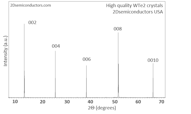
XRD data collected from WTe2 crystals (sharpest XRD peaks in the commercial market)

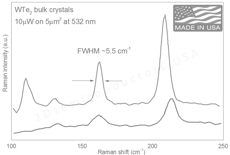
Raman spectrum collected from WTe2 crystals (also sharpest and most defined Raman signal from commercial WTe2 crystals)

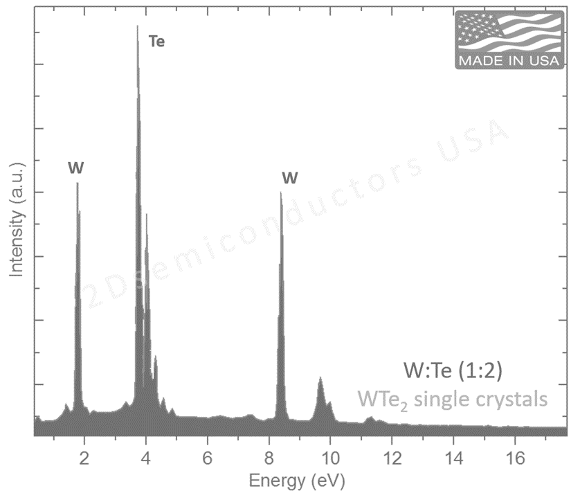
EDS spectrum collected from WTe2 crystals

Partial List of Published Articles Using Our WTe2 Crystals (as of 2017)
L. A. Walsh et. al. "WTe2 thin films grown by beam-interrupted molecular beam epitaxy" 2Dmaterials, 4, 2 (2017)
P. Lu et.al. Origin of superconductivity in the Weyl semimetal WTe2 under pressure, Phys. Rev. B. 94, 224512 (2016)
M. Kim et. al. Determination of the thickness and orientation of few-layer tungsten ditelluride using polarized Raman spectroscopy, 2D Materials, Volume 3, Number 3
Y. Kim. et.al. Anomalous Raman scattering and lattice dynamics in mono- and few-layer WTe2, Nanoscale, 2016,8, 2309-2316
Additional Information
Elements: |
W,Te |
Element: |
Tungsten |
Element: |
Tellurium |
Formula: |
WTe2 |
Material class: |
MX2 |
Material class: |
Dichalcogen |
Material class: |
Quasi-1D |
Properties: |
Metal |
Properties: |
Superconductor |
Properties: |
Semimetal |
Growth method: |
CVT |
Growth method: |
Flux |
Doping: |
Undoped |


