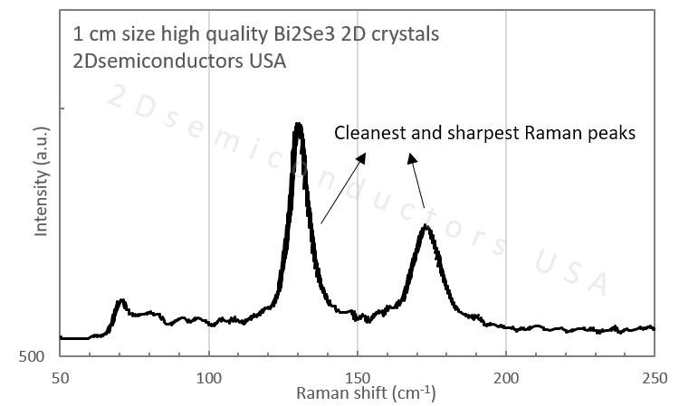
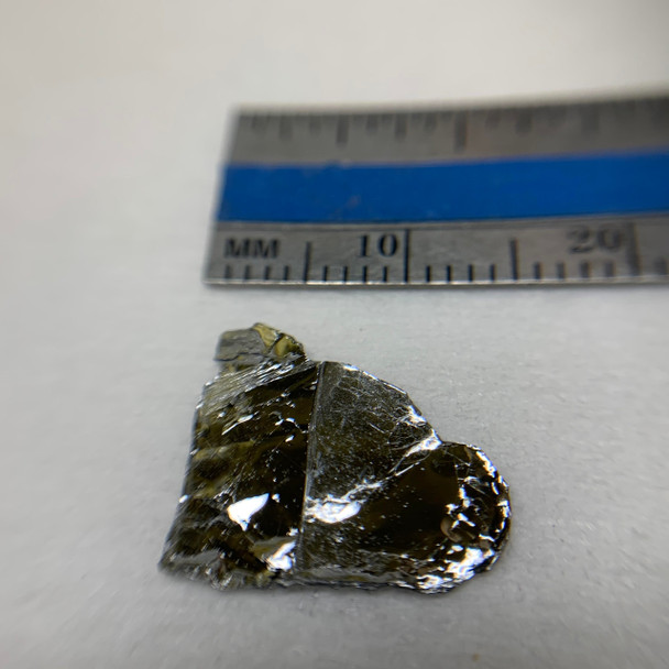
Bi2Se3 crystals: 1 cm large size high quality 2D crystals - 2Dsemiconductors USA Raman spectrum on Bi2Se3 crystals: 1 cm large size high quality 2D crystals - 2Dsemiconductors USA XRD from Bi2Se3 crystals: 1 cm large size high quality 2D crystals - 2Dsemiconductors USA Properties of Bi2Se3 crystals: 1 cm large size high quality 2D crystals - 2Dsemiconductors USA

Bi2Se3 crystal

SKU: BLK-BI2SE3-CVT
$590.00

World's largest commercially available electronic grade Bi2Se3 crystals.

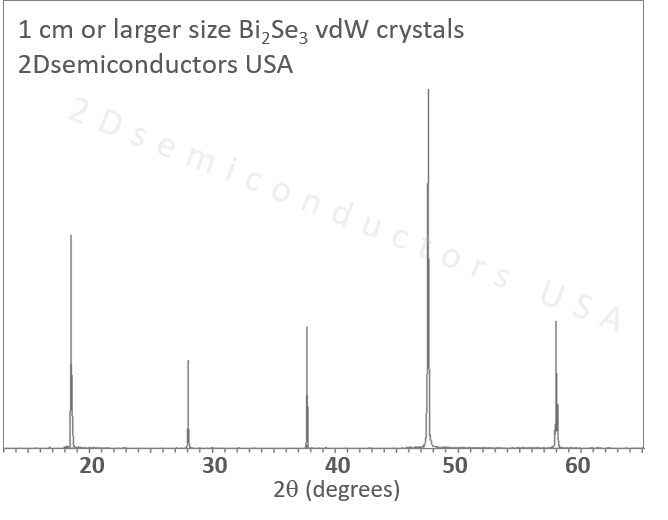
We offer guaranteed largest undoped or doped Bi2Se3 crystals in the commercial market. Bismuth selenide (Bi2Se3) is a topological insulator crystal belonging to metal chalcogenide material group. Similar to transition metal dichalgonides and graphite, Bi2Se3 is a layered material with weak vdW interlayer coupling. Our Bi2Se3 crystals have been developed at our facilities with topological states, structural crystallinity, reduced defect density, and high purity in mind. They measure ~1cm in size which is the largest size offered in the field. Our crystals exhibit world only 99.9999% purity levels and defect density concentrations as low as 1E9cm-2. Our Bi2Se3 crystals are ideal for electronic, topological insulator, and other solid state sciences research. Examples include scanning tunneling (STM), transmission electron microscopy (TEM), and other spectroscopic studies. Overall, Bi2Se3 displays very sharp and clear Raman modes with FWHM less than 4cm-1, sharp XRD pattern free of minority phases. If your research needs doping in Bi2Se3, we can also incorporate Ca, Nb, Ni, and Au dopants in Bi2Se3 crystals. Please also see our doped p-type and n-type Bi2Se3 crystals.

Typical characteristics of Bi2Se3 crystals 

Sample size World's largest size commercially available crystals. Larger than centimeter >1cm 
Properties

Topological insulator

Crystal structure and Exfoliation characteristics

a=b=c=0.41 nm c=2.853 nm, a=b=90, g=120

Very easy to exfoliate

Production method Bridgman growth (Highest purity 6N pure) Optional: CVT grown (less pure)


XRD data collected from Bi2Se3 crystals - 2Dsemiconductors USA
bi2se3-crystals-xrd-ii.png

Raman spectrum of Bi2Se3 crystals

bi2se3-crystals-raman.png


Example publication from this product 

L. A. Walsh et. al. "Fermi Level Manipulation through Native Doping in the Topological Insulator Bi2Se3" ACS Nano, 12 (6), pp 6310–6318 (2018)

Full Description
Formula: Bi2Se3
Qty
  • Description

    Bi2Se3 crystal

    World's largest commercially available electronic grade Bi2Se3 crystals.

    We offer guaranteed largest undoped or doped Bi2Se3 crystals in the commercial market. Bismuth selenide (Bi2Se3) is a topological insulator crystal belonging to metal chalcogenide material group. Similar to transition metal dichalgonides and graphite, Bi2Se3 is a layered material with weak vdW interlayer coupling. Our Bi2Se3 crystals have been developed at our facilities with topological states, structural crystallinity, reduced defect density, and high purity in mind. They measure ~1cm in size which is the largest size offered in the field. Our crystals exhibit world only 99.9999% purity levels and defect density concentrations as low as 1E9cm-2. Our Bi2Se3 crystals are ideal for electronic, topological insulator, and other solid state sciences research. Examples include scanning tunneling (STM), transmission electron microscopy (TEM), and other spectroscopic studies. Overall, Bi2Se3 displays very sharp and clear Raman modes with FWHM less than 4cm-1, sharp XRD pattern free of minority phases. If your research needs doping in Bi2Se3, we can also incorporate Ca, Nb, Ni, and Au dopants in Bi2Se3 crystals. Please also see our doped p-type and n-type Bi2Se3 crystals.

    Typical characteristics of Bi2Se3 crystals 

    Sample size World's largest size commercially available crystals. Larger than centimeter >1cm 
    Properties

    Topological insulator

    Crystal structure and Exfoliation characteristics

    a=b=c=0.41 nm c=2.853 nm, a=b=90, g=120

    Very easy to exfoliate

    Production method Bridgman growth (Highest purity 6N pure) Optional: CVT grown (less pure)


    XRD data collected from Bi2Se3 crystals - 2Dsemiconductors USA

    bi2se3-crystals-xrd-ii.png

    Raman spectrum of Bi2Se3 crystals

    bi2se3-crystals-raman.png


    Example publication from this product 

    L. A. Walsh et. al. "Fermi Level Manipulation through Native Doping in the Topological Insulator Bi2Se3" ACS Nano, 12 (6), pp 6310–6318 (2018)